PCB DFM vs DFA engineering comparison showing fabrication verification, assembly review, BOM validation, XYRS analysis, and PCB CAM engineering workflow.

PCB DFM vs DFA Engineering: Understanding the Key Differences

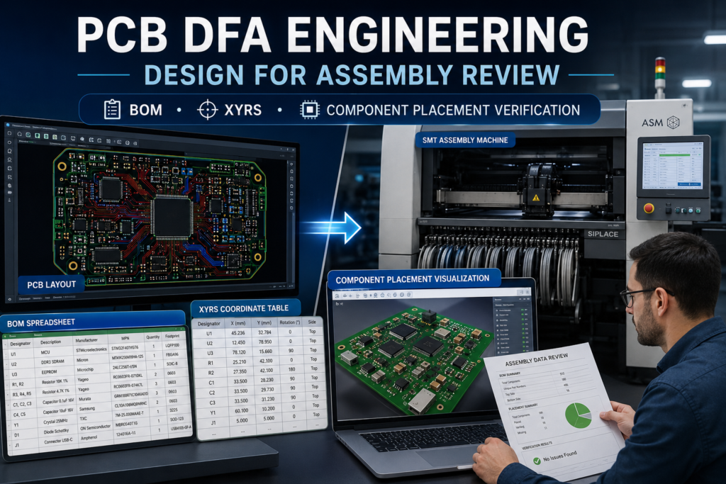
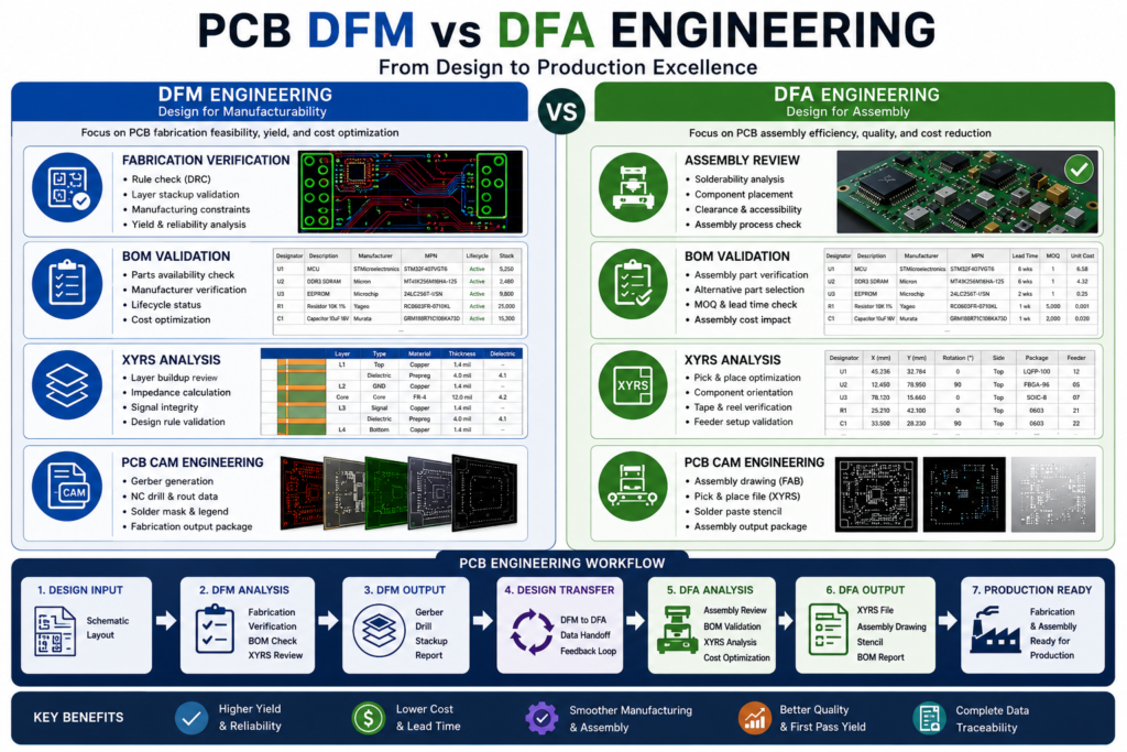
Introduction Understanding PCB DFM vs DFA is essential for successful PCB manufacturing and assembly. In PCB manufacturing, two critical engineering processes help ensure successful production: Design for Manufacturing (DFM) and Design for Assembly (DFA). Although these terms are often used together, they focus on different stages of the manufacturing process. Understanding the difference between PCB […]

What Is PCB DFA Engineering?

Understanding Design for Assembly in PCB Manufacturing PCB DFA (Design for Assembly) Engineering is the process of evaluating a printed circuit board design to ensure it can be assembled efficiently, accurately, and reliably during the PCB assembly process. While PCB CAM engineering focuses on fabrication readiness, DFA engineering focuses on assembly readiness. The goal is

PCB CAM Engineering

DFM Checks Every PCB Designer Should Know | PCB Design for Manufacturing Guide

DFM Checks Every PCB Designer Should Know | PCB Design for Manufacturing Guide Introduction Design for Manufacturing (DFM) is one of the most important stages in PCB production. A PCB design may function perfectly electrically, but if it cannot be manufactured reliably, production problems and delays become inevitable. DFM analysis helps ensure that PCB layouts

PCB CAM Engineering

Top 10 Gerber File Mistakes That Delay PCB Manufacturing

Top 10 Gerber File Mistakes That Delay PCB Manufacturing Introduction Gerber files are the foundation of PCB manufacturing. Even small errors in Gerber data can cause production delays, manufacturing defects, or complete fabrication failures. Many PCB issues occur not because of bad circuit design, but because the manufacturing files were incomplete, inconsistent, or improperly prepared.

Professional PCB CAM Engineering

What is PCB CAM Engineering?

What is PCB CAM Engineering? Introduction PCB CAM Engineering is one of the most critical stages in the printed circuit board manufacturing process. CAM stands for Computer-Aided Manufacturing, and PCB CAM engineers are responsible for converting PCB design data into manufacturing-ready production files. Before a PCB enters fabrication, the design must be checked, optimized, and

Scroll to Top